Pn Junction Diode - what happens to carrier profiles when voltage biases are applied?
The pn Diode Circuit Symbol and Terminal Characteristics(6.1)
There are 3 regions of operations of the pn diode
Zero Bias- diode current \(I_D>0\) with the diode voltage \(V_D\approx 0.7 v\)
Forward bias- diode current \(I_D\approx 0\)
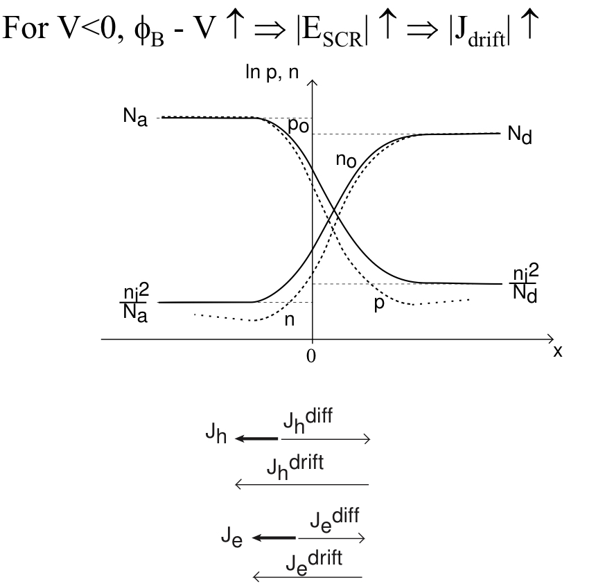
Backward Bias- diode current \(I_D<0\) and the diode voltage \(V_D< V_{BD}\) where \(V_{BD}\) is the diode’s breakdown voltage

The transport of holes from the p side across the depletion region into the n side under a forward bias is called hole injection
The transport of electrons from the n side to p side of the junction under a forward bias is called electron injection
Let us see what is happening in the different regions
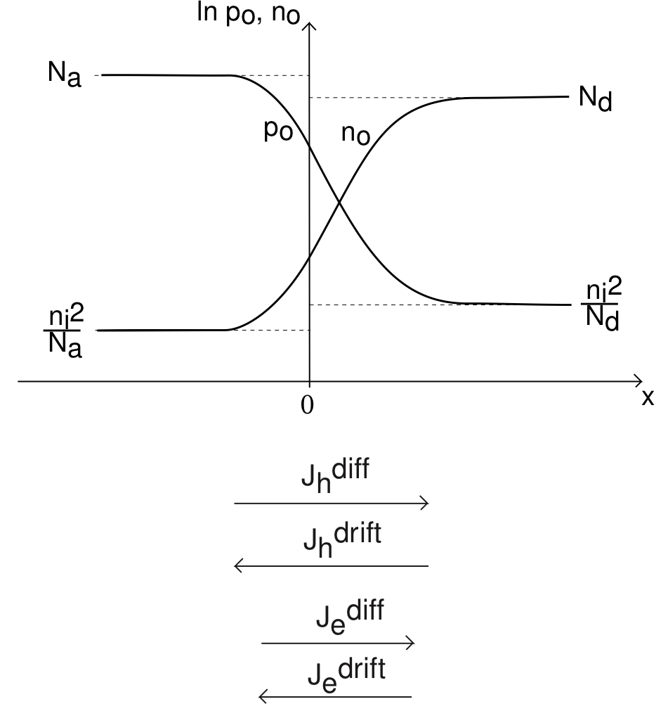
We have \[|J_\text{drift}| = |J_\text{diff}|\]

We have \[|J_\text{drift}| < |J_\text{diff}|\] This means we have a net diffusion current in the space charge region or into the QNRs
Net diffusion hole current \(J_h\) to the right
Net diffusion electron current \(J_e\) to the left
Both of which in the direction of the SCR towards the ohmic contacts
We have \[|J_\text{drift}|>|J_\text{diff}|\] This means we have a net drift current in the space charge region or from the QNRs
Net drift hole current \(J_h\) to the left
Net drift electron current \(J_e\) to the right
Both of which in the direction of away from ohmic contacts into the SCR
To sum up
In forward bias: injected minority carriers diffuse through QNR and recombine at semiconductor surface
In reverse bias, minority carriers generated at the semiconductor surface diffuse through the QNR and extracted by SCR


Comments
Post a Comment